
Besides current mirrors and basic amplification stages like common-source, common-gate, and source-follower amplifiers, the differential pair is considered one of the most important circuit blocks in analog design. Unlike basic amplifier stages, the differential stage has two signal inputs of opposite signs, allowing it to amplify a differential input signal, which is a tremendous advantage for most applications. Another aspect, often overlooked, is that biasing a basic amplifier stage always requires a reference current, introducing noise into the signal path. This is not the case for a differential stage, where noise from reference currents appears differentially and is canceled. Finally, the differential input stage enables many amplifier configurations, such as inverting amplifiers with defined gain via feedback, non-inverting amplifiers, integrators, differentiators, filters, and many more.
However, the aim of this article is not to describe applications for a differential pair. Instead, we will focus on sizing the transistors of a differential pair to meet a given specification. As a first step, we will perform circuit analysis to understand how the amplifier functions. We will provide a more practical solution rather than a detailed circuit analysis that considers all contributors to the transfer function. Regarding \(DC\) open-loop gain, the situation is similar to the common-source amplification stage, with the difference that we have two transistors consuming half the current but contributing equally. Therefore, the same expression as for the single-sided common-source amplifier is applicable, hence, we will get
$$\begin{equation}
A_{0} = -\frac{g_{mPM0}}{g_{DSPM0}+g_{DSNM0}}
\end{equation}$$
We should mention that the drain-source resistance of the current source providing the supply current to the differential pair is not relevant. From a differential perspective, the common node of the two input transistors does not move, making it equivalent to a ground node.
As for the frequency-dependent open-loop gain, we have a similar situation as with the common-source stage. The dominant pole, which acts as a low-pass filter, is determined by the total capacitance connected to the output node — typically equivalent to the load capacitor — and the total resistance connected to ground. In our case, in the absence of a load resistance, the total resistance is the drain-source transconductances of the transistors connected to the output node. This yields in
$$\begin{equation}
f_{p} = \frac{g_{DSPM0}+g_{DSNM0}}{2 \pi C_{DNM0}}=\frac{g_{mPM0}}{2 \pi A_0 C_{DNM0}}
\end{equation}$$
In this expression, we have already introduced the open-loop gain, which makes it easy to derive the unity gain frequency. The open-loop gain must be higher than the dominant pole frequency, as long as no other pole or zero is introduced. Hence, we obtain
$$\begin{equation}
f_{u} = f_p A_0 = \frac{g_{mPM0}}{2 \pi C_{DNM0}}
\end{equation}$$
As more devices are involved in the circuit, more nodes will be required. Each node can have its own set of independent or dependent transconductances and parasitic capacitors (while neglecting inductors in our consideration). These conductances and capacitors may create poles and zeros. In general, poles shunt away energy from a node with increasing frequency, proportional to \(1/\omega\). Zeros increase energy in a node with increasing frequency, proportional to \(\omega\).
Another practical rule of thumb is that poles and zeros, which lie one to two decades apart in terms of angular frequency, can be treated independently. Here, SizingTool3 is of great help, as it allows quick estimation of the order of magnitude of transconductances and parasitic capacitors and therefore helps to approximate the location of poles and zeros.
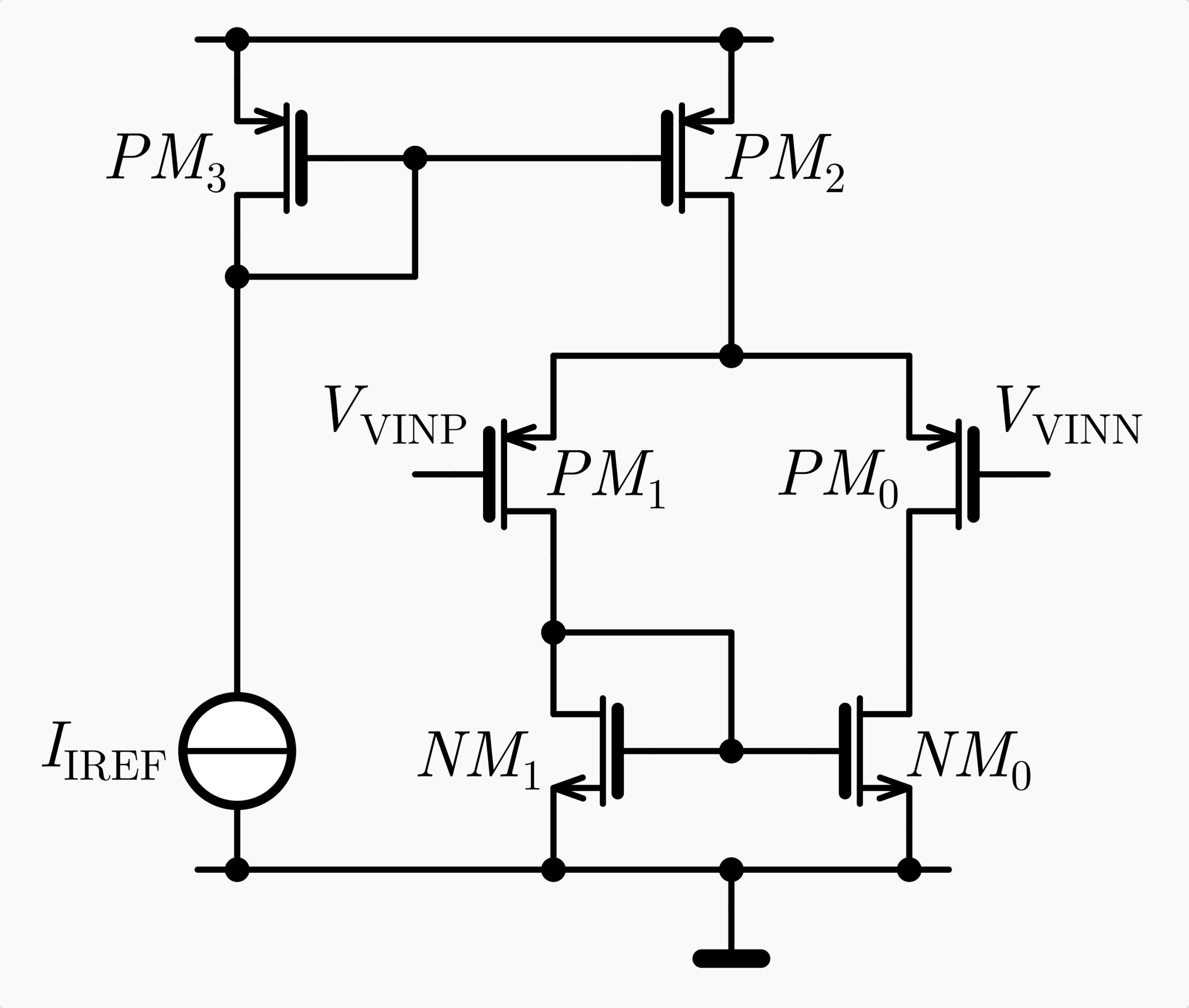
In that sense, we will find a pole at the gate of the n-channel transistor \(NM_0\). Since transistor \(NM_1\) is diode-connected, it creates a path to ground with conductance \(g_{mNM1}\). This, combined with the total parasitic capacitance \(C_{GNM0}\) connected to the gate of \(NM_0\), forms a pole at
$$\begin{equation}
f_{p2} = \frac{g_{mNM1}}{2 \pi C_{GNM0}}
\end{equation}$$
Since the transconductances \(g_{mPM0}\) and \(g_{mNM1}\) are of similar order of magnitude, but \(C_{GNM0}\) is significantly smaller than \(C_{DNM0}\), this second pole \(f_p\) is generally at a much higher frequency than the unity gain frequency \(f_u\).
The pole at the gate of transistor \(NM_1\) will reduce the signal energy originating from node VINP. Consequently, the output signal or voltage at drain node of transistor \(NM_1\) will decrease. However, this reduction has a limit, which occurs when the entire signal energy from \(V_{VINP}\) is shunted away, resulting in the output signal magnitude being halved. In this context, one can argue that at twice the frequency \(f_u\) , an opposite effect occurs, which does not reduce the output signal but rather counteracts the signal reduction. The counteraction of a signal pole in signal transmission is, obviously, a zero. Therefore, this effect creates a zero at twice the unity gain frequency.
Following the concept that a zero will increase energy in a node, the capacitor \(C_{GDNM0}\) will lead energy into the output node at the drain of \(NM0\). A zero appears when the current in the channel of \(NM0\), which is equal to \(V_{GSNM0} \times g_{mNM0}\), is equal to the current flowing through the capacitor \(C_{GDNM0}\), which is approximately equal to \(V_{GSNM0} \times \omega\). Solving for the frequency yields
$$\begin{equation}
f_{zRHP} = \frac{g_{mNM0}}{2 \pi C_{GDNM0}}
\end{equation}$$
However, following the previous argument, the location of the zero is significantly higher than the unity gain frequency \(f_{u}\).
Finally, the signal output magnitude cannot drop to zero. At a certain frequency, the transfer function from input to output will be dominated by the capacitive divider formed by the gate-drain capacitance of transistor \(PM_0\) and the total capacitance at the output node, which is basically the load capacitor. This magnitude is further reduced by -6 dB, since only half of the input signal is available. Consequently, the minimum gain calculates to (multiply the expression below times 0.5)
$$\begin{equation}
A_{0min} = \frac{C_{GDPM0}}{C_{GDPM0}+ C_{DNM0}}
\end{equation}$$
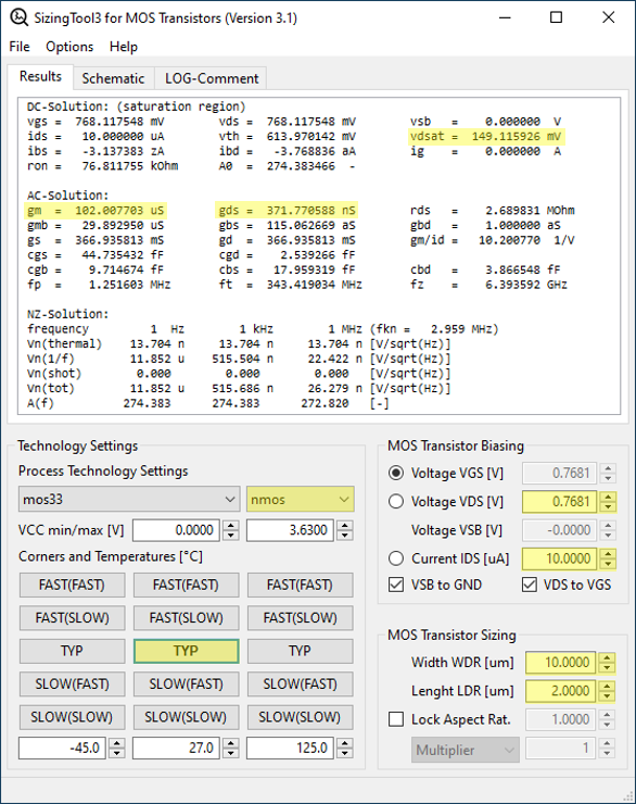
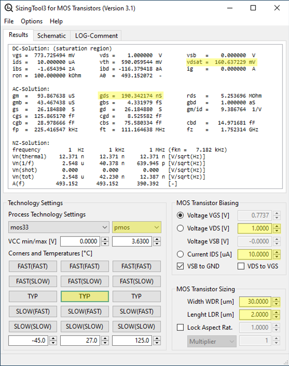
Due to the lack of specifications in this example, we will consider the same transistor sizing as in the example given for the common-source amplifier. The corresponding results for the transistor pairs \(PM_0\) and \(PM_1\), as well as \(NM_0\) and \(NM_1\), are given below. One could argue that the values are chosen to achieve a large output swing while still maintaining a reasonable open-loop gain. Design goals can be manifold. Another design goal could be to minimize the overall noise. We will discuss this case later in a dedicated blog on Miller-OTA amplifiers.
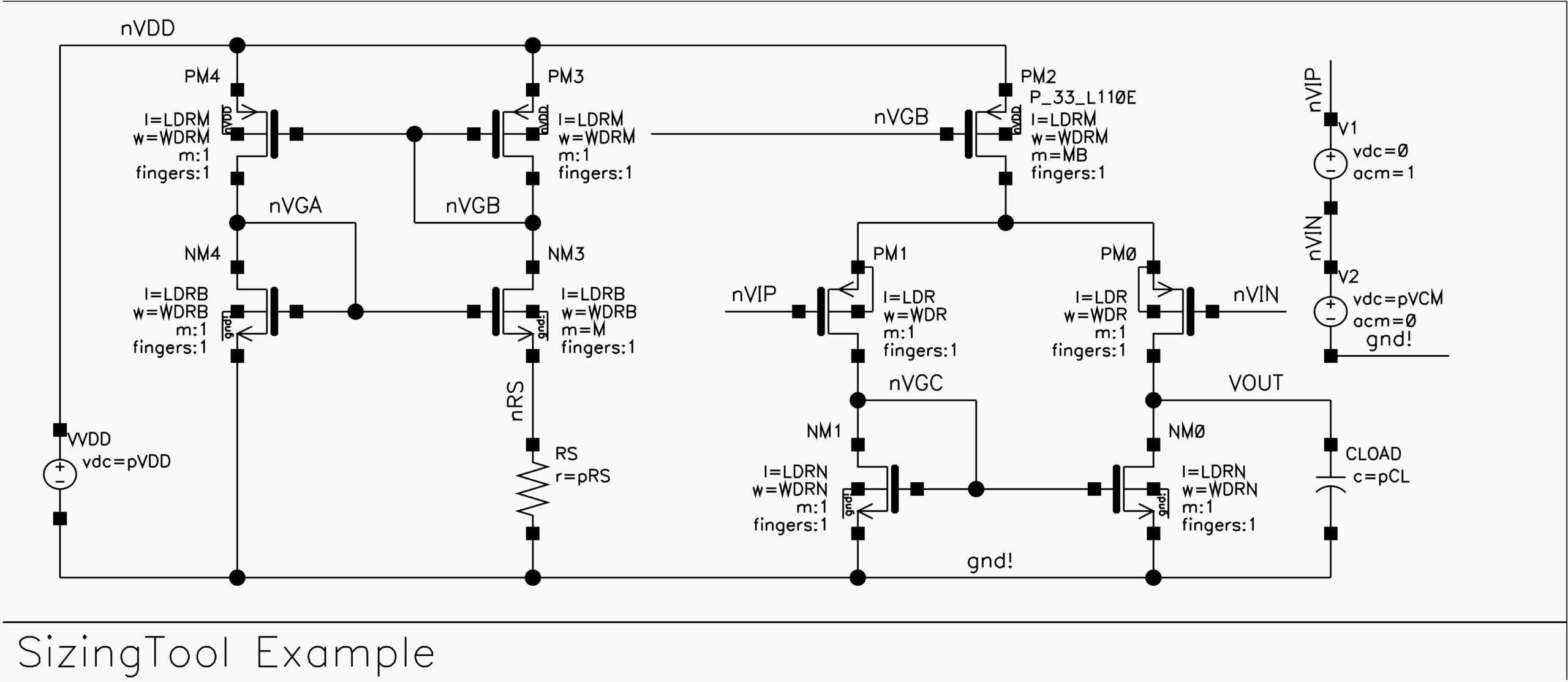
For the verification, we have chosen a simple test-bench configuration, as shown below. We will create the reference biasing current using a constant \(g_m\) biasing circuit to account for different process corners. For the \(DC\) output voltage, we expect it to be equal to the gate voltage of transistor \(NM_0\) due to symmetry and the absence of imperfections such as offset voltages. Therefore, no special action needs to be taken regarding the input common voltage, similar to the example of a common-source amplifier.
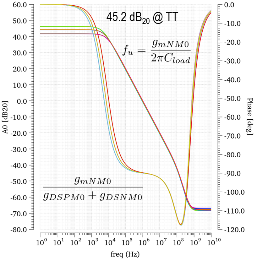
The simulation results presented in the figure below are based on transistor sizing as determined using SizingTool3. The load capacitor was chosen such that, with a transconductance of transistor \(PM_0\) of 100\(\mu\)S, a unity gain bandwidth of 1MHz was achieved, resulting in a value of 15.915pF. As in the example of the common-source amplifier, the open-loop gain is expected to be around 45\(dB_{20}\), as predicted by SizingTool. Additionally, with a gate-drain capacitor of approximately 8.5fF for transistor \(PM_0\), the minimal open-loop gain is expected to be approximately 71\(dB_{20}\). Furthermore, the total parasitic capacitance at the gate node of transistor \(NM_0\) is predicted by SizingTool to be around 200fF. This results in a frequency for the second pole of around 80 MHz, as confirmed by the simulation. The related zero, therefore, is around 160MHz, but it is not explicitly seen since it coincides with the gain limitation due to the gate-drain capacitance of transistor \(PM_0\). The zero due to the gate-drain capacitance of transistor \(PM_0\) is expected to be somewhere around 6.4 GHz, hence, irrelevant.
Leave a Reply