
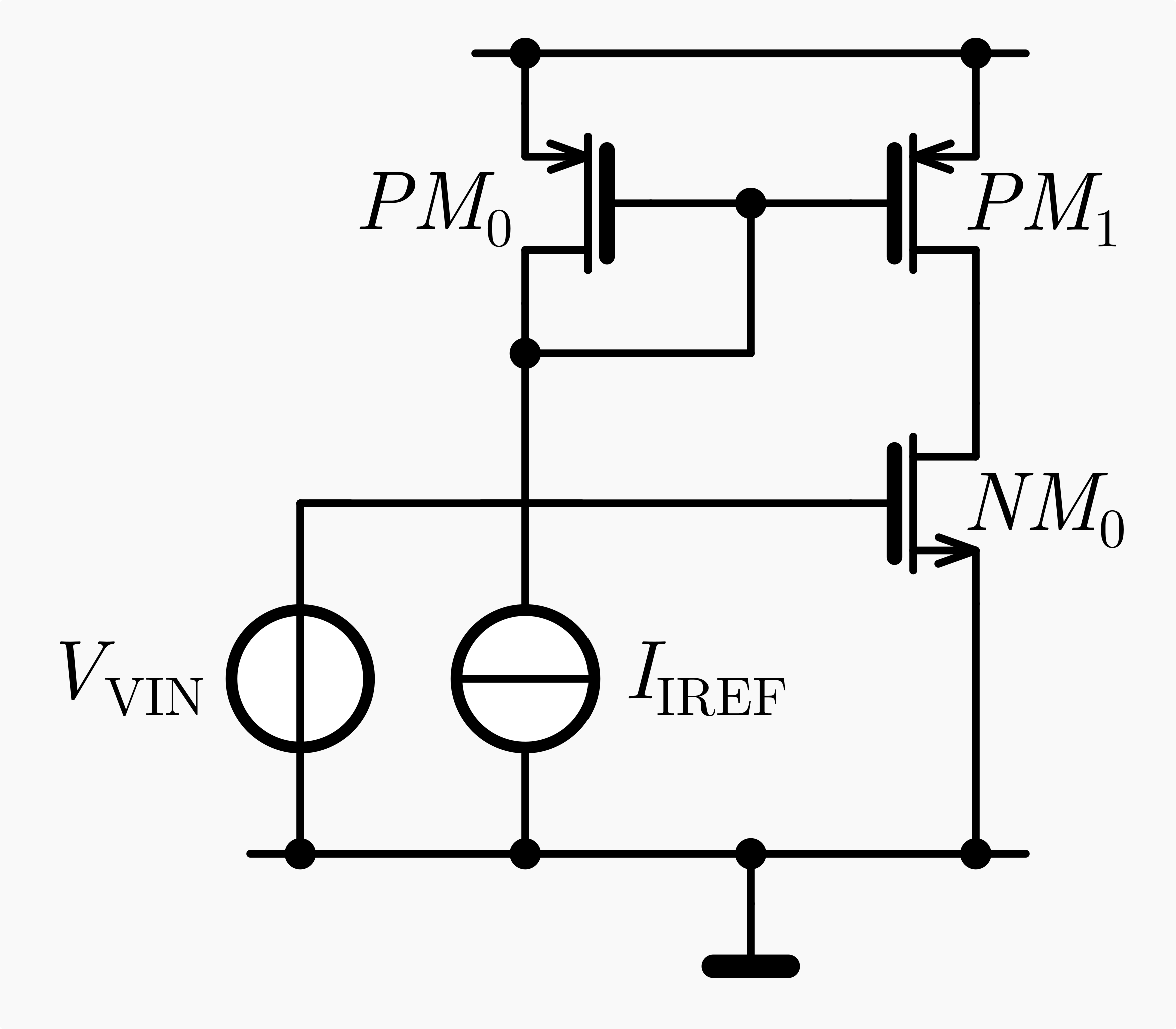
A common application of simple current mirrors is in single stage amplifiers with an active load. This common-source configuration (see Fig. 1) is highly favored as a gain stage, especially when high input impedance is desired. The term “common source” refers to the common node between the input and output voltages, which is the source terminal. In this example we use an n-channel transistor as the amplifier and a p-channel transistor as the active load. The p-channel transistor delivers a controlled bias current to the amplifier transistor. This active load acts as a current source, providing a high impedance output load without the need for a large resistor.
Here we take a pragmatic approach to analyzing the transfer function, rather than delving into a detailed analysis that includes all the parasitic capacitances in the circuit. This approach is generally sufficient for practical analogue design. However, you are encouraged to explore the detailed calculations. You will find that for most low frequency applications the additional poles and zeros derived are significantly greater than our operating bandwidth and can therefore be neglected. By performing a circuit analysis, we can quickly determine the small signal open loop gain of the amplifier at \(DC\). This gain is characterized by the transconductance gm, which converts the input voltage into a current. This current then produces an output voltage across the amplifier’s output resistance. The \(DC\) open loop gain can be described as
$$\begin{equation}
A_{0} = -\frac{g_{mNM0}}{g_{DSPM0}+g_{DSNM0}}
\end{equation}$$
where the output resistance is represented by the inverse of \(g_{DSPM0}+g_{DSNM0}\). This amplifier has a dominant pole at the output node. Consequently, the frequency of the pole, specifically its angular frequency, is determined by the time constant formed by the output load capacitance (not shown in the schematic) and the output resistance. The dominant pole can therefore be expressed as
$$\begin{equation}
f_{p} = -\frac{g_{DSPM0}+g_{DSNM0}}{2\pi C_{load}}
\end{equation}$$
We are dealing with a first order linear system from a small signal perspective. Therefore, the frequency dependent open loop gain will begin to decrease at the pole frequency, decreasing by a factor of ten each decade. Consequently, at a frequency that is higher than the pole frequency by a factor equal to the open loop gain \(A_0\), the total gain is reduced to unity. This frequency is known as the unity gain frequency and is given by
$$\begin{equation}
f_{u} = -\frac{g_{mNM0}}{2\pi C_{load}}
\end{equation}$$
Other poles and zeros will be neglected for the reasons mentioned above.
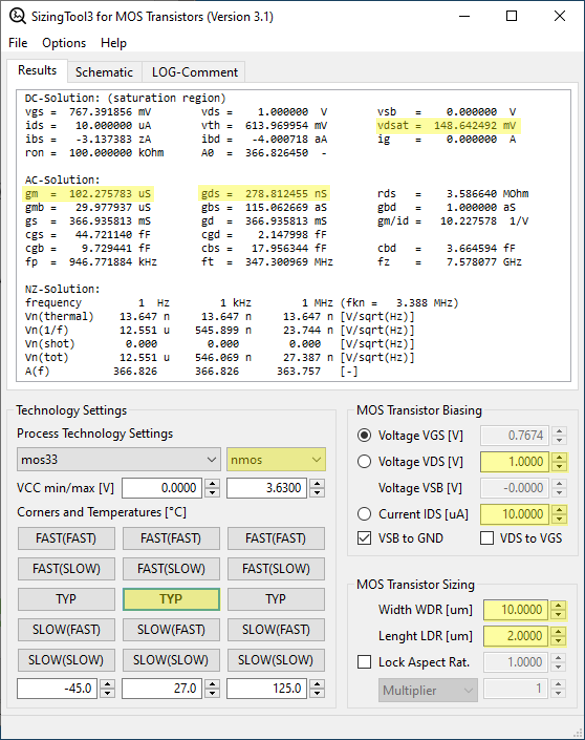
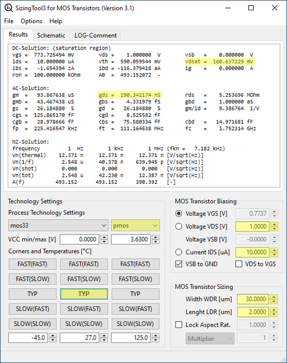
To give an example of how to dimension our common-source amplifier, we need to establish some specifications. Let’s say we want our amplifier to have a unity gain frequency of 10 MHz with a load capacitor \(C_L\) of \(100\mu S/(2\pi 10MHz)\). We would therefore need a transconductance gm of \(100 \mu S\) to meet these specifications. Let’s also assume a supply voltage \(V_{DD}\) of 2V and we want the output voltage to be in the range of 0.5 V to 1.5 V. The open loop gain in our example should be 40 \(dB_{20}\).
Based on the open-loop gain relationship, we need an output impedance to accommodate the output transconductances \(g_{ds}\) of the transistors, with values less than 500 nS if evenly distributed. In addition, we assume that the saturation voltage Vdsat should be around 200 mV, considering a 200 mV to 300 mV margin to the minimum drain-source voltage \(V_{DS}\) of 0.5V for the n-channel and p-channel transistors. Both characteristics can be adjusted by the length of the transistors according to the following relationships
$$\begin{equation}
V_{eff} = V_{GS}-V_{T} \approx V_{dsat}
\end{equation}$$
$$\begin{equation}
V_{eff} \propto \sqrt{\frac{I_{DS}}{W}} \propto \sqrt{L}
\end{equation}$$
$$\begin{equation}
g_{ds} = -\frac{\partial I_{DS}}{\partial V_{DS}} \propto \lambda I_{ds} \propto \frac{1}{L}
\end{equation}$$
Therefore, we need to select an appropriate current density \(I_{DS}/W\) and adjust the transistor length until the values of \(g_{ds}\) and \(V_{dsat}\) meet the specified requirements. In our example, we chose a current density of 1 \(\mu A/\mu m\) for the n-channel transistor and 1/3 \(\mu A/\mu m\) for the p-channel transistor and achieved \(g_{ds}\) values less than 300 nS and \(V_{dsat}\) around 150 mV for typical conditions. While you can invest more effort in optimizing these values further, it’s important to consider process variations, shifts in biasing currents, and other non-idealities. Optimizations within a 20% margin are generally acceptable. Once you are satisfied with the results, you can adjust the width of the n-channel transistor while maintaining the current density constant until you achieve the desired transconductance. This adjustment will not alter \(V_{dsat}\) or \(g_{ds}\), as the current density and transistor length remain unchanged. Finally, adjust the width of the p-channel transistor so that the drain current \(I_{DS}\) provides the correct biasing current for the amplifier. Similarly, the current density will remain unchanged during this process. Fig. 2 and Fig. 3 illustrate the corresponding settings for the above examples.
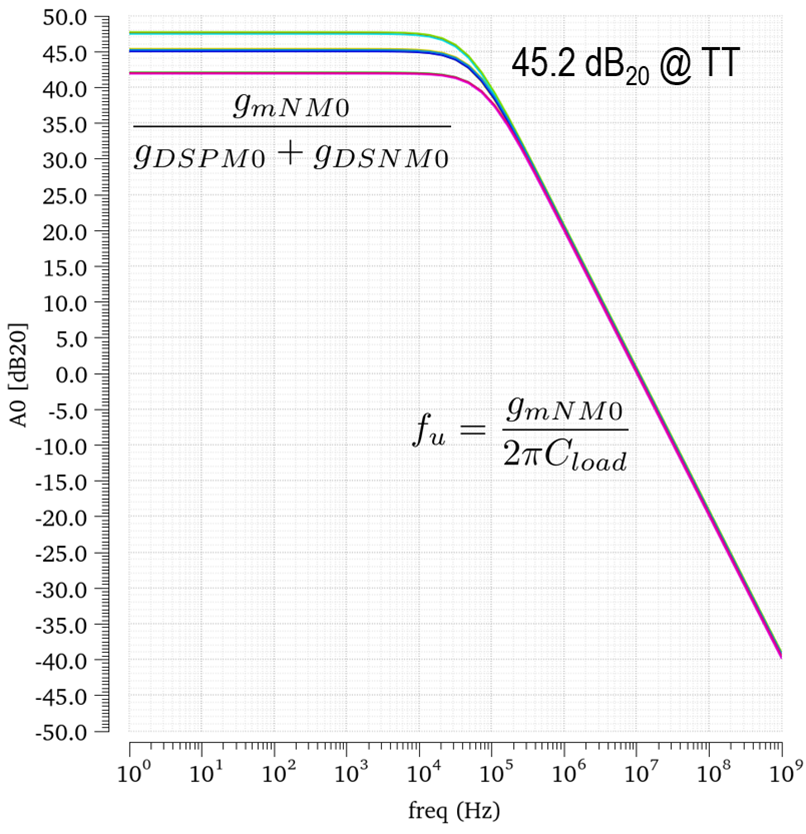
Given these values, we would expect an open-loop gain of around 46 \(dB_{20}\) under typical conditions. Regarding the output conductance, you can adjust the drain-source voltage \(V_{DS}\) accordingly in the tool and verify that none of the output conductances exceed 500 nS. Additionally, the unity gain frequency \(f_u\) is determined by the transconductance \(g_m\). If a constant-\(g_m\) biasing scheme is used, the unity gain frequency \(f_u\) will remain unchanged across different process corners. Conversely, the open-loop gain will vary, as the output conductance is related to the threshold voltage of the transistors, which is process-dependent.
At this point, the sizing of the amplifier is complete. This simple example demonstrates that the entire process is deterministic, requiring only adjustments to our tool inputs until the desired outputs are achieved. The design process included simplified circuit analysis and the use of the SizingTool. In this procedure, the output conductance \(g_{ds}\) and the transconductance \(g_m\) could be adjusted independently, preventing loops of readjustment. Furthermore, this design process provides a comprehensive understanding of the circuit, as all properties of the transistors are always visually available.
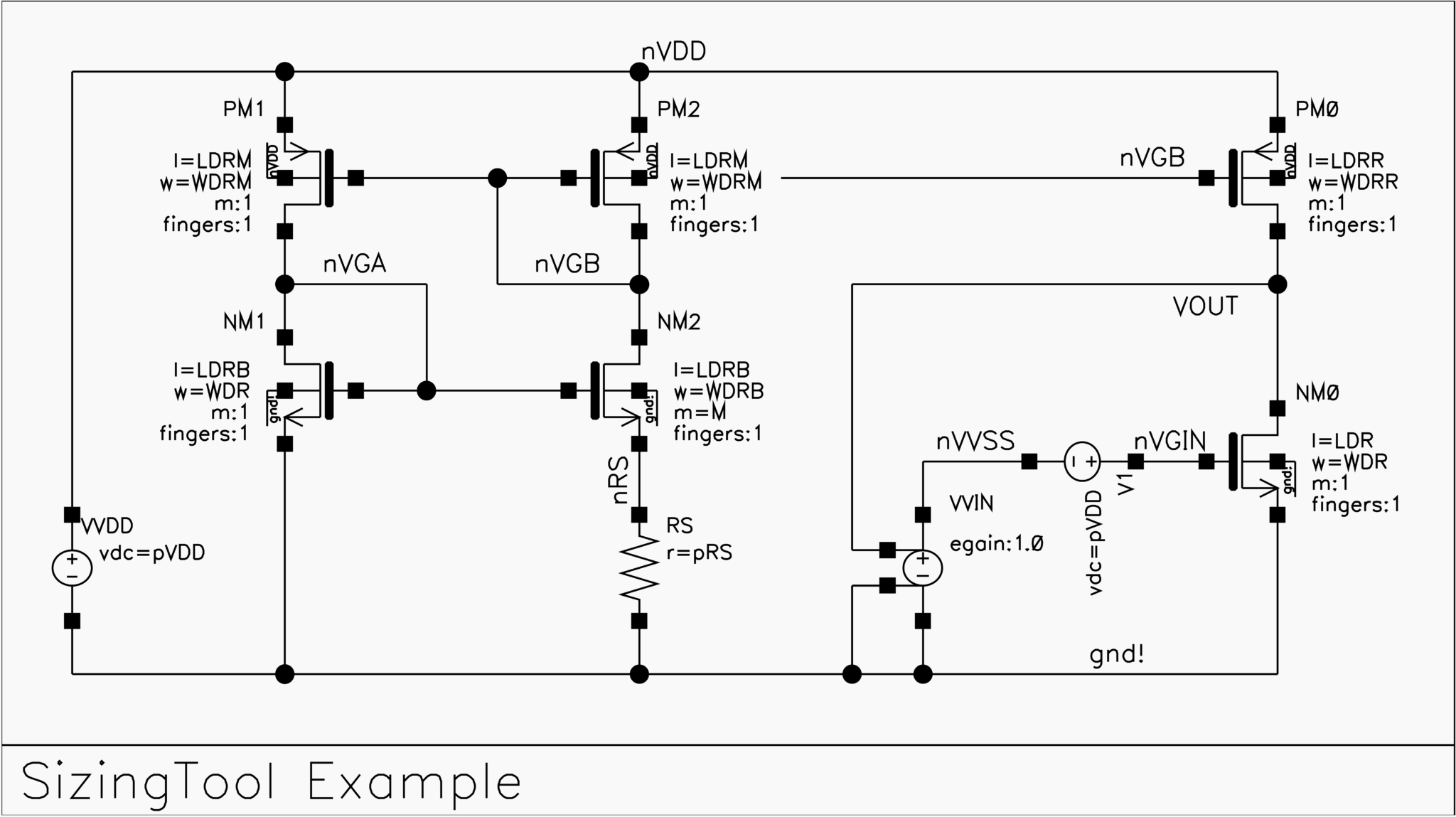
To verify our amplifier stage, we use a commercial simulation tool. However, to set the amplifier in the proper operation mode, we need to bias the active load and apply the correct \(DC\) voltage at the input of the amplifier, specifically at the gate node of the n-channel transistor (see Fig. 4). To provide the correct settings for the p-channel active load, we replicate the constant gm-biasing circuit, which additionally allows us to maintain an approximate transconductance across all process corners.
To set the appropriate gate voltage for the n-channel transistor, we use a feedback loop from the output node. In the given schematic, this is realized with a voltage-controlled voltage source. In the example, the loop gain is set to one, so the voltage source could be omitted. However, the testbench becomes more generalized, allowing easy adjustment of other feedback ratios.
In the case of unity gain feedback, it becomes clear that the n-channel transistor is in a diode-connected configuration. Hence, the input or output voltage corresponds to the gate-source voltage, which is around 0.6 V. If the output voltage needs to shift to another value, a series source can be used to establish the corresponding shift.
In Fig. 5, the waveform of the transfer function over frequency is shown. As expected, the transconductance (gm) remains constant, so the unity gain frequency stays unchanged at 10 kHz across different process corners, as desired. For the open-loop gain \(A_0\), the amplification does not drop below 40 \(dB_{20}\), meeting the required specifications. You can further verify that the transfer characteristic remains stable by sweeping the \(DC\) output voltage between 0.5 V and 1.5 V, as required for the \(DC\) output voltage range.
It is worth mentioning that applying circuit analysis for an in-depth understanding, combined with the SizingTool and the constant current-density method, allowed us to size the amplifier correctly on the first attempt. Verification is then reduced to simply double-checking if the circuit meets the specifications. In this example, no further optimizations are required.
Leave a Reply