
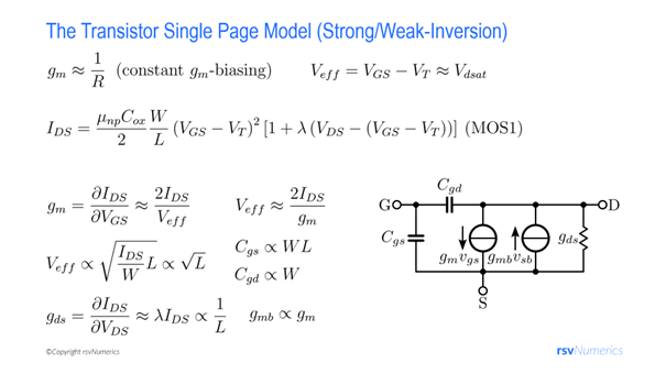
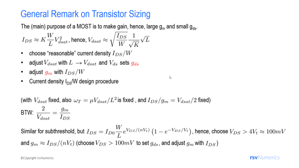
The purpose of a transistor for what it is invented for is to create gain. To do this it needs a large transconductance \(g_m\) and a small output conductance \(g_{ds}\). It would therefore be desirable to be able to adjust these small signal parameters \(g_m\) and \(g_{ds}\) independently of each other in the design of the transistor by the choice of the appropriate width and length. This can be done using the constant current density technique.
The output conductance \(g_{ds}\) is defined by the drain-source saturation voltage \(V_{dsat}\) and the actual operating point of the drain-source voltage \(V_{ds}\). Thus, \(V_{dsat}\) defines the voltage at which the drain current as a function of the source-drain voltage \(I_{ds}(V_{ds})\) flattens out, and the drain-source voltage \(V_{ds}\) defines the margin to the same voltage. In practise, the drain-source voltage \(V_{ds}\) should be approximately et least \(200 mV\) higher than the voltage \(I_{ds}(V_{ds})\). From the square law model we learn
$$\begin{equation}
I_{ds} \approx K \frac{W}{L} V_{dsat}^2 \text{, hence, }V_{dsat} \approx \sqrt{\frac{I_{ds}}{W}} \frac{1}{\sqrt{K}} \sqrt{L}
\end{equation}$$
with \(K\) as the gain-factor. Here, if \(\sqrt{I_{ds}/W}\), known as the current density in the transistor channel, is reasonably chosen and kept constant, we can adjust the saturation voltage \(V_{dsat}\) to the desired value by choosing an appropriate length \(L\). Also, adjusting drain-source saturation voltage \(V_{ds}\) or transistor width \(W\) while keeping \(\sqrt{I_{ds}/W}\) constant, does not change the \(V_{dsat}\). In case \(V_{dsat}\) cannot be set to the desired value, the current density \(\sqrt{I_{ds}/W}\) must be adjusted accordingly.
In this sense, the expression for the transconductance \(g_m\) described by the square law model can be rearranged as following
$$\begin{equation}
g_{m} =\frac{2 I_{ds}}{(V_{gs}-V_{TH})} \approx \frac{2 I_{ds}}{V_{dsat}} = 2 \sqrt{K \frac{W}{L} I_{ds}} = 2 W \sqrt{K} \sqrt{\frac{I_{ds}}{W}} \frac{1}{\sqrt{K}} \sqrt{L}
\end{equation}$$
Here, changing the width \(W\) while keeping the current density \(\sqrt{I_{ds}/W}\) and length \(L\) constant, will change the transconductance \(g_m\) proportionally, while not affecting the saturation voltage \(V_{dsat}\) as explained above. Hence, the constant current density method allows to set transconductance \(g_m\) and output conductance \(g_{ds}\) independently.
Further, while controlling the drain-source saturation voltage \(V_{dsat}\) by keeping the voltage fixed, keeps the transit frequency \(\omega_T = \mu V_{dsat}/L^2\) and \(g_m/I_{ds} = 2/V_{dsat}\) at the same value as well.
Similarly, the constant current method is applicable to the sub-threshold operation of a MOS-transistor. However, the expression for the drain-source current given as
$$\begin{equation}
I_{DS} = I_{D0} \frac{W}{L} e^{V_{GS}/(nV_{th})} \lbrace 1 – e^{-V_{DS}/(V_{th})} \rbrace
\end{equation}$$
lacks a threshold voltage, and consequently voltage \(V_{dsat}\). Here, the thermal voltage is expressed as \(V_{th} = kT/q\). In sub-threshold, the drain-source saturation voltage is replaced by the ‘normalised’ transconductance \(g_m/I_{ds}\). Numerically, the correspondence of \(2/V_{dsat} = g_m/I_{ds}\) given in the saturation mode of the transistor is approximately maintained in the subthreshold mode. Therefore, we can choose a \(g_m/I_{ds}\) by adjusting an appropriate length \(L\) for a given current density \(I_{ds}/W\). Now, the given ‘normalised’ transconductance \(g_m/I_{ds}\) guarantees sub-threshold operation, and as long as the drain-source voltage is \(V_{ds} > 4 V_th \approx 100 mV\), we can expect a high output transconductance (in the drain-source current relation, the term \(1- exp(-V_{ds}/(nV_{th}))\) is close to 1, so \(g_{ds}\) will be very large). Similar to the saturation regime, we can adjust the output conductance \(g_{ds}\) with length \(L\) at constant current density \(I_{ds}/W\).
Next we adjust the drain current \(I_{DS}\) or equivalently the width \(W\) at constant current density \(I_{ds}/W\). As we saw above, this will not affect the operating point of the transistor, so \(g_m/I_{ds}\) or \(g_{ds}\) will remain the same. However, adjusting the drain current \(I_{ds}\) will increase \(g_m = I_{ds}/(n V_{th})\). Again, as for the saturation mode, in the subthreshold mode, the width \(W\) can adjust the transconductance \(g_m\) at constant \(I_{ds}/W\), while \(g_m/I_{ds}\) or \(g_{ds}\) are not affected.
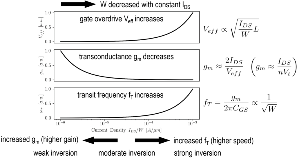
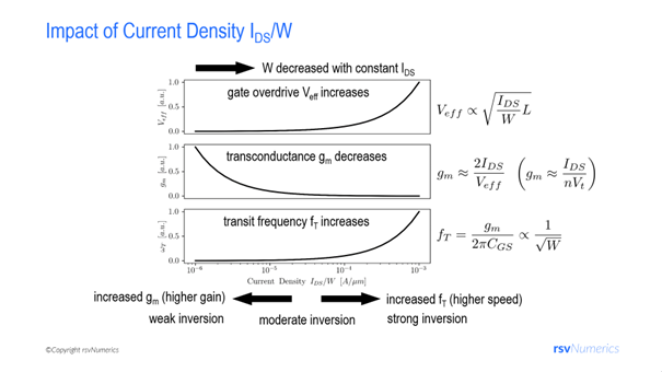
In Fig. 1 an overview is given, how current density \(I_{ds}/W\) affects drain-source saturation voltage \(V_{dsat} \approx V_{eff} = V_{GS} – V_{TH}\), transconductance \(g_m\), and transit frequency \(\omega_T = 2 \pi f_T\).
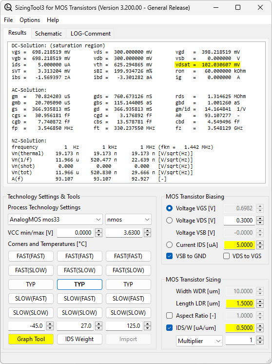
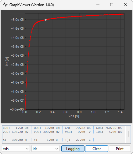
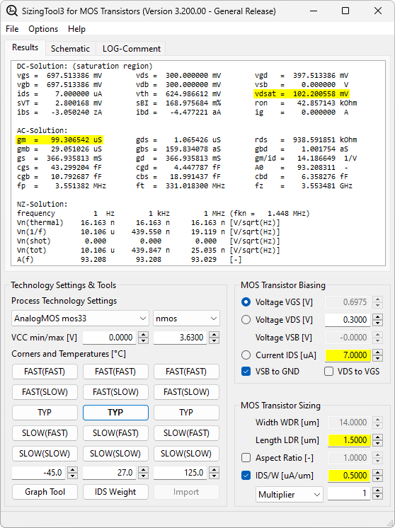
SizingTool3 provides a convenient method for selecting the correct dimensions of a MOS-transistor for given specifications such as transconductance \(g_m\), output conductance \(g_{ds}\), intrinsic gain \(A_0\), etc. In this example, we assume that previous analysis has shown that we need a transistor that operates so that it provides a transconductance \(g_m\) of \(100 \mu S\) at a drain-source voltage \(V_{ds}\) of \(300 mV\) and a reasonable output conductance \(g_{ds}\) to achieve an intrinsic gain \(A_0 \approx 100\). We conclude that the output region of the transistor requires a \(V_{dsat} = 100 mV = V_{ds} – 200 mV\). As shown in Fig. 2, we select in SizingTool3 the voltage \(V_{DS} = 0.3 V\), the current \(I_{DS} = 5.0 \mu A\), and adjust the length \(L_{DR}\) and the ratio \(I_{DS}/W\) until \(v_{dsat}\) and \(A_{0}\) give the correct value. Using the GraphViewer (see Fig. 3) we see that at \(V_{DS} = 0.3 V\) the \(I_{DS}(V_{DS})\) has flattened out and will give a reasonable output conductance \(g_{ds}\). Next we increase the current \(I_{DS}\) until the transconductance \(g_m\) shows the correct value of \(100 \mu S\). As shown in Fig. 4, a current of \(I_{DS} = 7.0 \mu A\) and a width \(W\) and length \(L\) is the correct choice for the transistor. The procedure can be repeated at different process corners and junction temperatures to ensure the correct specification is achieved over all PVT’s (Process – Voltage – Temperature). Further, you can select the ‘Lock Aspect Ratio’ option and readjust dimensions (w/o affecting \(g_m\), \(g_{ds}\)) in order to meet additional requirements such as noise or parasitic capacitors.
Get the cheat-sheets:
Leave a Reply